Reverse engineering of ARM microcontrollers
Texas Instruments TM4C123G
Introduction
Microcontrollers are small processing units that are widely used in todays electronics. MCUs are usually used for very specific and dedicated tasks. Therefore, they are usually very limited in resource aspects (speed, memory) to reduce their cost and make them more reliable. They are found in many critcal fields of technology such as automotive, space industry or medical devices.
Key characteristics of microcontrollers:
- small build-in RAM and ROM
- in many cases no operating system
- interrupts
Reverse engineering of the MCU firmware is different from a typical ARM binary. There is no header for IDA to recognize sections and segments, no file system, all the memory space is flat. Hardware specific operation and very low level hardware interoperation makes reversing an MCU firmware more complicated. This article explains one of the approaches a researcher can take to successfully load an MCU firmware into IDA Pro and start reversing. The process is described based on the Texas Instruments Tivia C series board and one of the labs available on EDX in the course “Embedded Systems - Shape The World: Microcontroller Input/Output”. A “hello world” example in the Microcontrollers’ world.
The processes of obtaining a firmware from the chip is out of scope of this article.
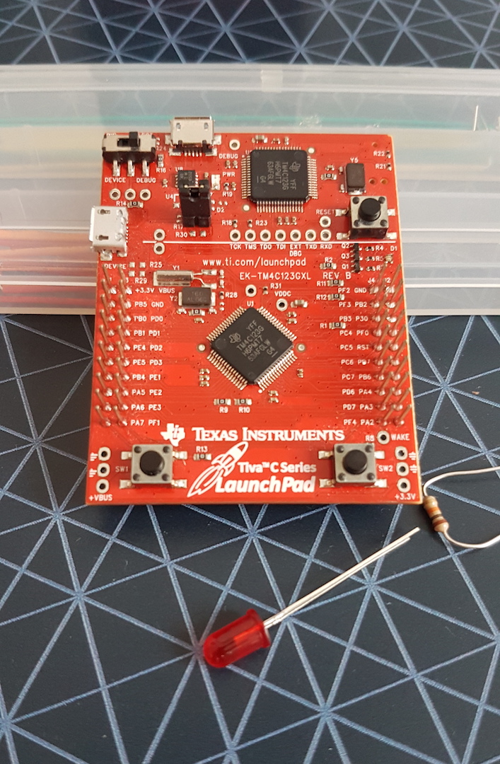
Texas Instruments Tivia C series Launchpad:
Loading firmware to IDA Pro
Firmware of the MCU is usually a flat binary file. It means there are no ELF (or similar) files that can be easily recognized by IDA. Therefore, to load the firmware some steps need to be taken.
When loading the binary firmware IDA greets with a window:
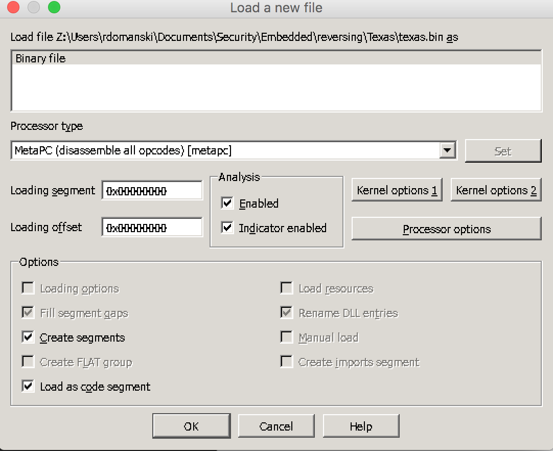
At this stage IDA is unable to recognize the file. Little help is needed :)
My first step is to identify the type of processor of the target. Looking at the datasheet for Texas Instruments TM4C123G MCU overview:
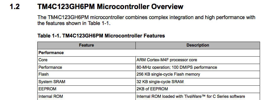
So the MCU is an ARM Coretex-M4F and wiki page provides more information about the ARM processor:
Key features of the Cortex-M4 core are:
- ARMv7E-M architecture
- 3-stage pipeline with branch speculation.
- Instruction sets:
- Thumb-1 (entire)
- Thumb-2 (entire)
- 1 to 240 interrupts, plus NMI.
- 12 cycle interrupt latency.
Now the information about the endianness. Searching the datasheet for ‘endian’ this can be found: All instruction and data memory accesses are little endian.
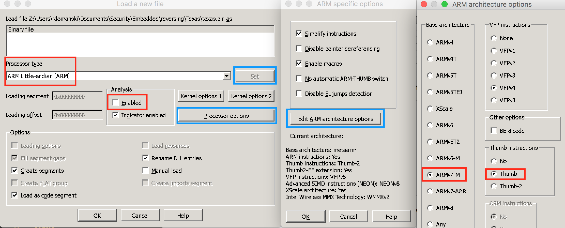
With this information following steps can be taken:
- Processor type can be set to ARM Little-endian [ARM]
- Click Set button and subsequently Processor options and Edit ARM architecture options
- Set Base architecture to ARMv7-M and Thumb In the Thumb instructions
- At this stage I tend to disable the Analysis.
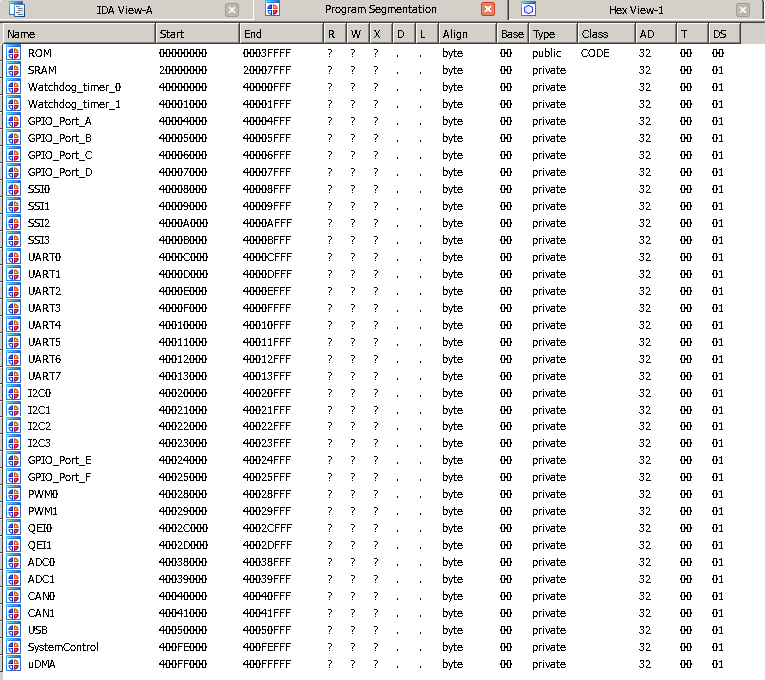
In the next step IDA asks for the RAM and ROM addresses. The actual values can be found in the datasheet again. It is usually referenced as ‘memory map’.
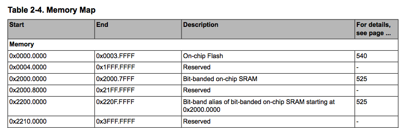
We know the start and end address (size) of the ROM and ROM sections. It it not uncommon to see that sections larger then the actual firmware but nevertheless I prefer to set it according to the datasheet specification as it helps in the reverse engineering process.
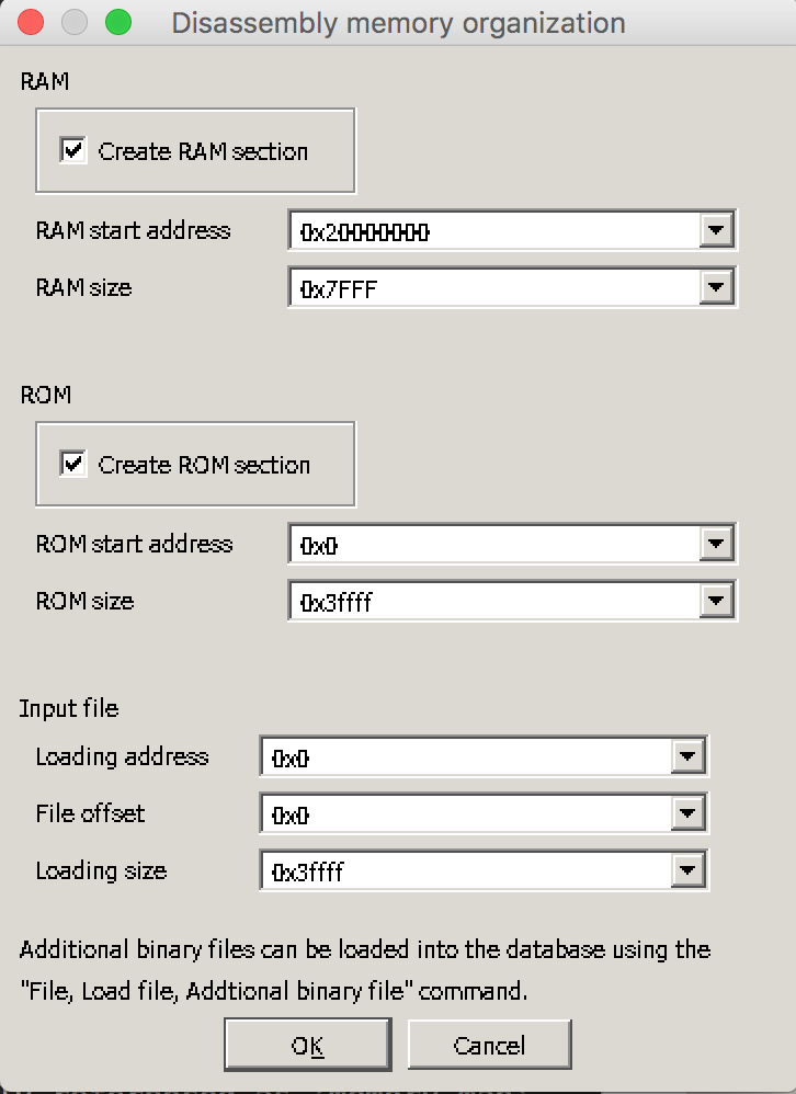
IDA loads and presents a loaded firmware in the ROM section.
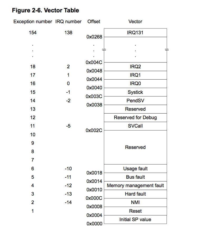
Vector Table
Microcontrollers implement special data structure called Vector Table. They are usually located at the start of the memory at 0x0000.0000 address. Its purpose is to manage exceptions handling. Reset is one of such an exception. Whenever the microcontroller powers-up, the Reset exception is called. The address located at the Reset vector is the first instruction that the CPU will execute.
Datasheets usually provide quite detailed description of the Vector Table. An example of Vector Table for Texas Instruments TM4C123G:
It confirms what is seen in IDA:
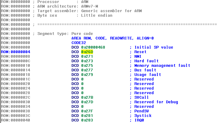
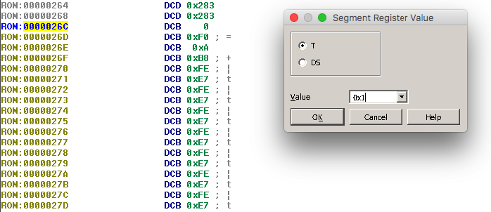
So the Reset handler points to the 0x26D as a first ARM instruction. But be careful! The first instruction is in fact at Offset 0x26C. As the manual states:
The least-significant bit of each vector must be 1, indicating that the exception handler is Thumb code
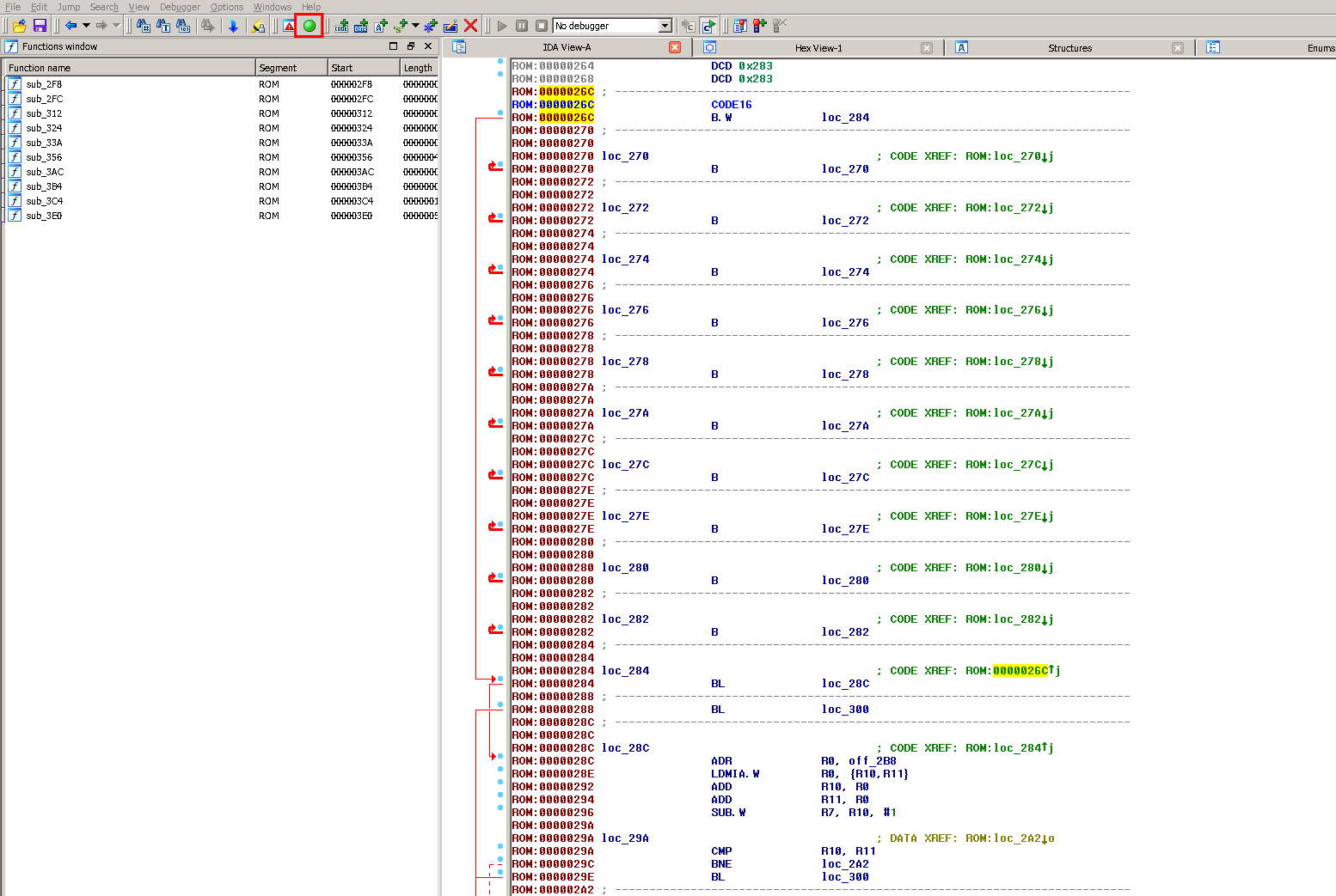
Having this in mind, it is required to mark the rest of the code as Thumb. Navigate to 0x26C and press alt-G. In the Segment Register Value select ‘T’ for Thumb and set Value to 0x1, which means Thumb mode enabled.
Now is the moment when I usually hit the autoanalysis button. And we have more familiar view of the IDA :)
Memory mapped I/O
Microcontrollers use the same address space for I/O devices and the memory. It means that when the program is performing read or write on the memory address it may be equal to read/write to the physical peripheral.
Example in IDA:
All the addresses of 0x400- are mapped to the peripherals. The list of memory regions is available in the datasheet. I wrote a script that creates segments to the corresponding peripherals. It simplifies reverse engineering. The script can be found in the github repository: segments.py.
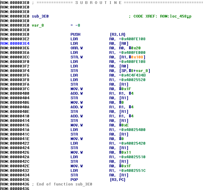
Lets focus on the first few instructions:
ROM:000003E2                 LDR             R0, =0x400FE108
ROM:000003E4                 LDR             R0, [R0]
ROM:000003E6                 ORR.W           R0, R0, #0x20
0x400FE108 address is loaded to the R0 register. It is known already that it is the memory region of “System Control”. To figure out what this address means it is required to read the datasheet again. Section for a “System Control” explains that the offstet 0x108 is pointing to “Run Mode Clock Gating Control Register 2” (RCGC2).
This register controls the clock gating logic in normal Run mode. Each bit controls a clock enable for a given interface, function, or module. If set, the module receives a clock and functions. Otherwise, the module is unclocked and disabled (saving power).
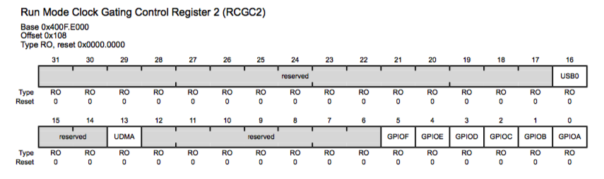
Note: I only have the legacy RO picture of the RCGC2 register.
Next instruction loads the value of the RCGC2 register (0x400FE108) into R0. Subsequently logical OR with value 0x20 is performed and the value is stored back in the 0x400FE108. It can be interpreted as providing a clock signal to the GPIO_F or in other words - enable the GPIO_F Port.
Logical OR instruction was used to perform a ‘non invasive’ bit setting. It is only needed to set one bit number 5 and leave all other bits in an unchanged state.
Rest of the instructions in this function do similar things - initialize the device. However, there is one part which is quite interesting to discuss.
ROM:00000416                 MOV.W           R0, #0xE
ROM:0000041A                 LDR             R1, =0x40025400
ROM:0000041C                 STR             R0, [R1]
0xE is loaded to R0. 0xE is 14 in decimal or 1110 in binary. The base address 0x40025000 is the GPIO_PORT_F. From the datasheet it can be read that the 0x400 offset is responsible for “GPIO Direction” setting.
The GPIODIR register is the data direction register. Setting a bit in the GPIODIR register configures the corresponding pin to be an output, while clearing a bit configures the corresponding pin to be an input. All bits are cleared by a reset, meaning all GPIO pins are inputs by default.
1 bit is representing 1 GPIO PIN. Therefore writing 0xE into the 0x40025400 sets pins PF1, PF2, PF3 of the GPIO_Port_F as output. PF0 is set as input. All other pins remain unchanged.
Reversing the main function
The main function of the microconroller presented in the graph mode:
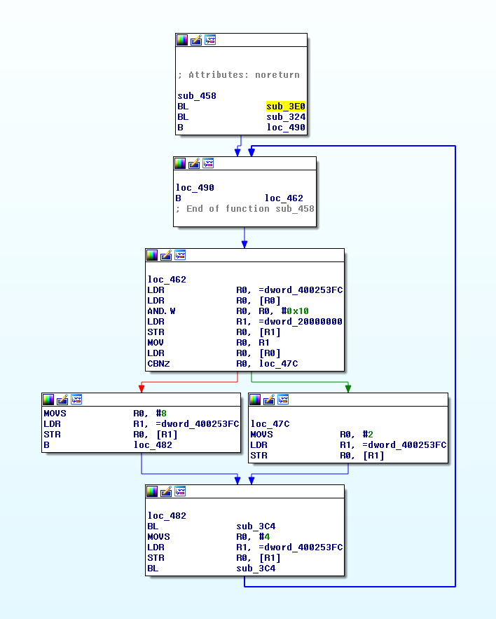
First, sub_3E0 function is called. This is the function that was explained in the previous section. The sub_324 can be skipped at this stage.
Next, there are some instructions performed in the loop with one conditional statement. The content of the loop starts with an interesting instructions:
ROM:00000462                 LDR             R0, =dword_400253FC
ROM:00000464                 LDR             R0, [R0]
ROM:00000466                 AND.W           R0, R0, #0x10
0x40025000 is the offset of the GPIO Port F register. However, the offset 0x000 - 0x400 is described as “GPIO Data”. This memory address range is used to read and write into the specific pins of the GPIO Port F. However, the read and write operation is performed using the “Bit specific addressing”.
Bit Specific Addressing
Bit Specific Addressing is a method to read (or write) the value of a specific or all bits with one instruction. All other pins are unaffected. Such a method is more efficient and simplifies the operation of the MCU.
In this example, the offset 0x3FC represents the pins which value is loaded to the R0. 0x3FC in binary is represented as ADDR[] = 0011.1111.1100. However, only ADDR[9:2] are used for the operation. It means that effectively binary 11.1111.11 is used to determine which bits to return, in this case, all of them.
For the sake of explanation, lets assume the ADDR[] = 0001.0110.1000 (0x168). It translates to ADDR[9:2] = 01.0110.10.
Bit7 - 0 -> no operation
Bit6 - 1 -> read/write
Bit5 - 0 -> no operation
Bit4 - 1 -> read/write
Bit3 - 1 -> read/write
Bit2 - 0 -> no operation
Bit1 - 1 -> read/write
Bit0 - 0 -> no operation
As a result operation on the memory address 0x40025168 would affect Bits 1, 3, 4, 6 of the GPIO PORT F.
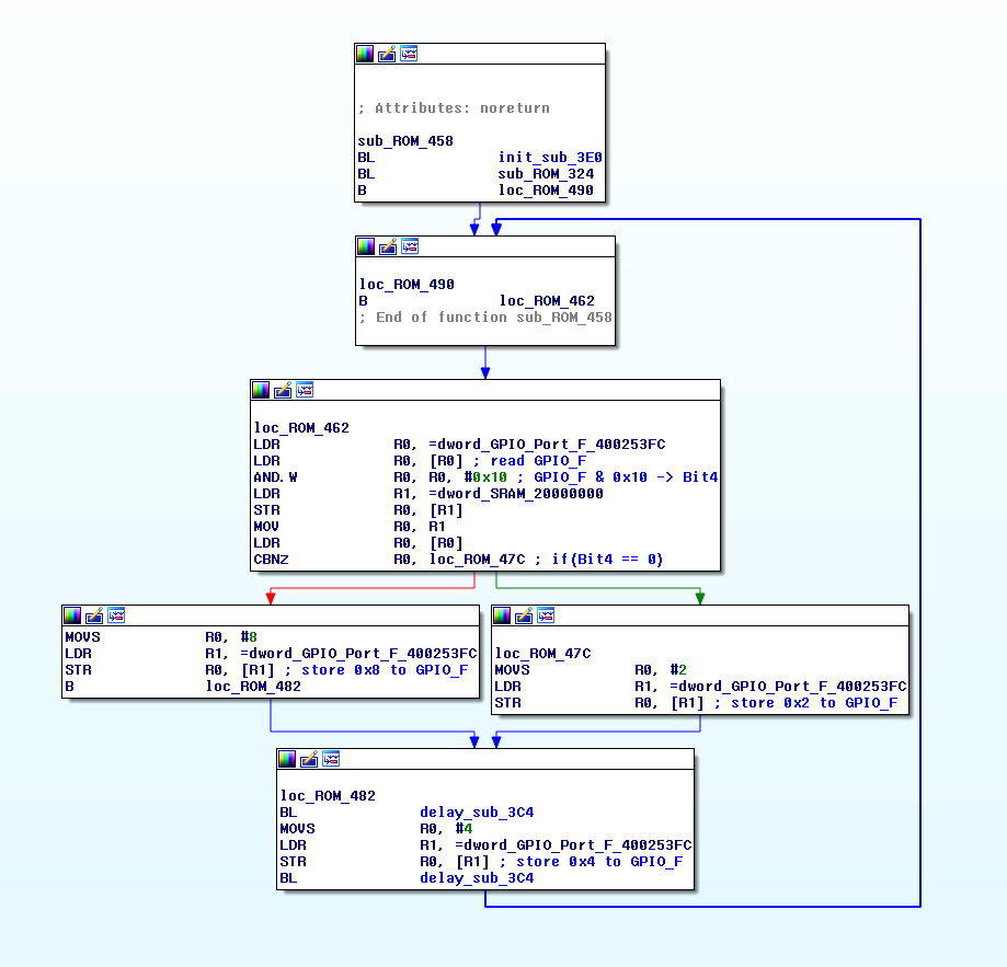
Now it is clear that the code is reading the status of all the pins of the GPIO Port F and it performs logical AND with 0x10. The logical AND is used to test if specific bit is set, in this case Bit4. Later on the compare operation is used and it branches depending on the Bit4, if it is 0 or 1. If Bit4 is 0 the program sets Port F to 0x2 else the PortF is set to 0x8.
At the end of the loop there is a call to sub_3C4 function. This function is not required to understand right now. (Spoiler: it’s a delay function) In the last basic block the Port F is set to 0x4 and the loop starts from the beginning.
Logic of the program
At this point the main function has been successfully reversed. It is clear what the instructions are doing - initializing pins, setting some pins, delaying instructions.
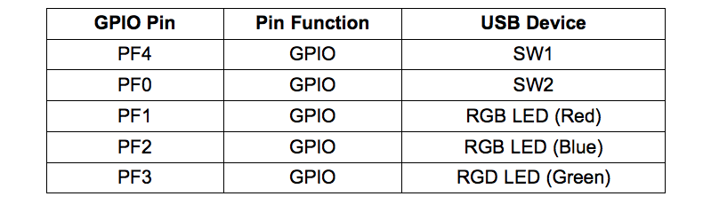
Such an information is only partially useful. Applying additional logic to what is known already would be helpful. The board that is being analyzed is the Texas Instruments Tiva C LaunchPad. It is a proto board with an ARM microcontroller. From the datasheet of the Tiva C board it can be read that the GPIO Port F is connected to the RGB LED and 2 physical switches.
This information sheds new light on the logic of the program. Same function as before but now with comments about the logic of the operation:
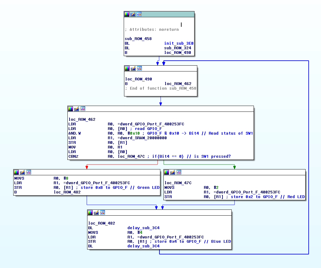
In short, the program reads the status of Switch1 (Pressed = 0, Unpressed = 1). If the SW1 is pressed the LED is turned Red. Otherwise the LED is turned Green. After the time delay is elapsed the LED is turned Blue. The loop starts from the beginning.
Summary
Reverse engineering of microcontroller firmware is a little bit different from reversing of ELF compiled binaries. IDA Pro will not understand the binary data by default. It also requires some knowledge how microcontroller works in order to recognize the special functionality in the assembly. Reading the chip’s datasheet is crucial as chips differ in functionality and build from each other.
The example presented here was a very simple one, can be seen as a “Hello World” of the microcontroller. Real world examples would be much more complex. Nevertheless, such an example is a good start to dive into the world of microcontrollers.
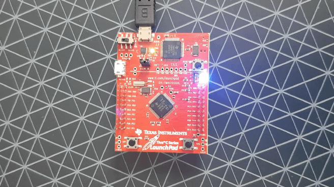
And the example of a working MCU: